- 您现在的位置:买卖IC网 > Sheet目录3871 > PIC18F84J11T-I/PT (Microchip Technology)IC PIC MCU FLASH 8KX16 80TQFP
PIC18F85J11 FAMILY
DS39774D-page 104
2010 Microchip Technology Inc.
8.6.2
16-BIT WORD WRITE MODE
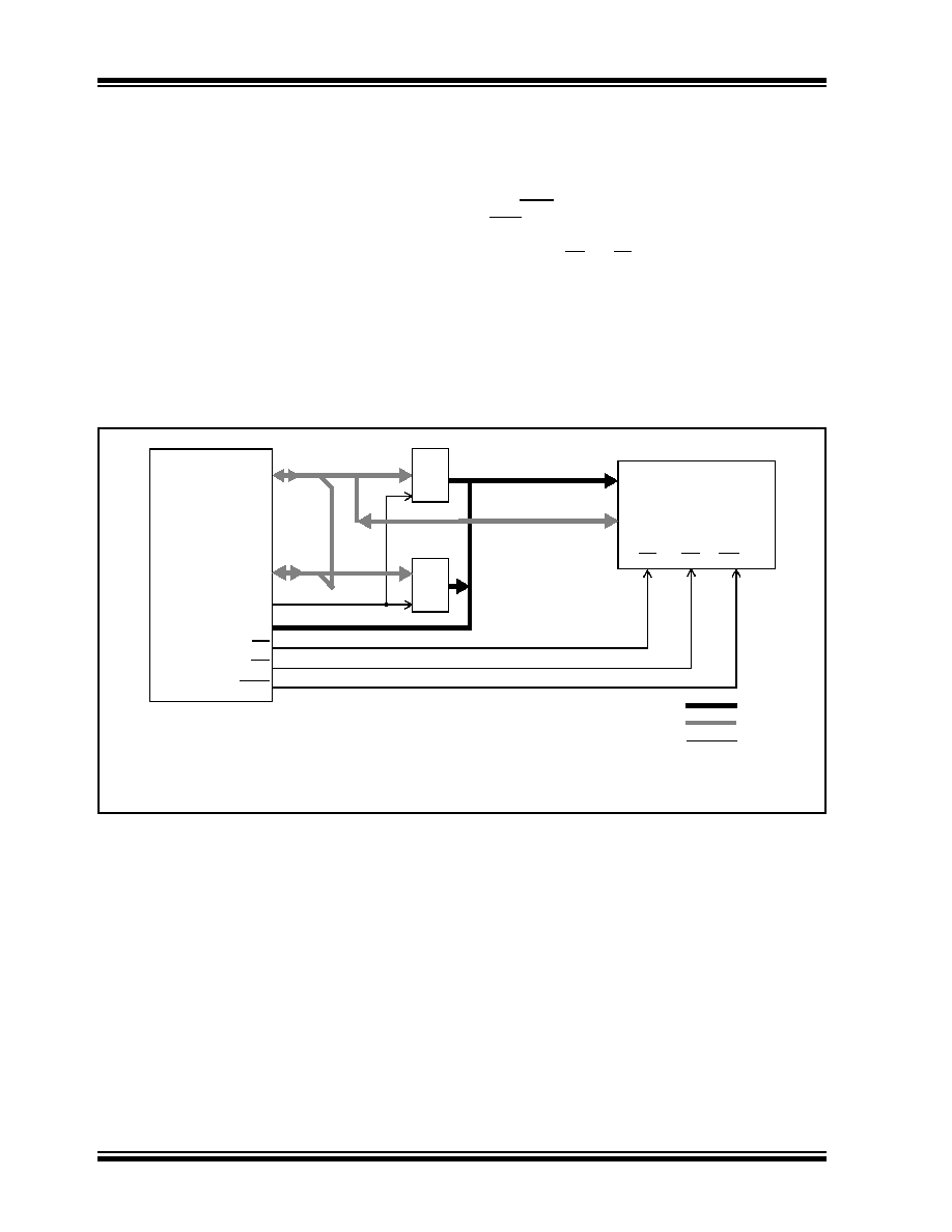
Figure 8-2 shows an example of 16-Bit Word Write
mode for PIC18F85J11 family devices. This mode is
used for word-wide memories which include some of
the EPROM and Flash-type memories. This mode
allows opcode fetches and table reads from all forms of
16-bit memory and table writes to any type of
word-wide external memories. This method makes a
distinction between TBLWT cycles to even or odd
addresses.
During a TBLWT cycle to an even address
(TBLPTR<0> = 0), the TABLAT data is transferred to a
holding latch and the external address data bus is
tri-stated for the data portion of the bus cycle. No write
signals are activated.
During
a
TBLWT
cycle
to
an
odd
address
(TBLPTR<0> = 1), the TABLAT data is presented on
the upper byte of the AD<15:0> bus. The contents of
the holding latch are presented on the lower byte of the
AD<15:0> bus.
The WRH signal is strobed for each write cycle; the
WRL pin is unused. The signal on the BA0 pin indicates
the LSb of the TBLPTR, but it is left unconnected.
Instead, the UB and LB signals are active to select both
bytes. The obvious limitation to this method is that the
table write must be done in pairs on a specific word
boundary to correctly write a word location.
FIGURE 8-2:
16-BIT WORD WRITE MODE EXAMPLE
AD<7:0>
PIC18F85J11
AD<15:8>
ALE
373
A<20:1>
373
OE
WRH
A<19:16>(1)
A<x:0>
D<15:0>
OE
WR(2)
CE
D<15:0>
JEDEC Word
EPROM Memory
Address Bus
Data Bus
Control Lines
Note 1:
The upper order address lines are used only for 20-bit address widths.
2:
This signal only applies to table writes. See Section 7.1 “Table Reads and Table Writes”.
CE
发布紧急采购,3分钟左右您将得到回复。
相关PDF资料
PIC18F24K22-I/SP
IC PIC MCU 16KB FLASH 28SPDIP
PIC18LF25K22-I/SO
MCU 8BIT 32KB FLASH 3.6V 28SOIC
PIC18F83J90T-I/PT
IC PIC MCU FLASH 4KX16 80TQFP
PIC18LF24K22-I/SP
IC PIC MCU 16KB FLASH 28SPDIP
PIC32MX110F016B-I/SS
IC MCU 32BIT 16KB FLASH 28SSOP
PIC18F85J50T-I/PT
IC PIC MCU FLASH 16KX16 80TQFP
PIC18F45J10-I/P
IC PIC MCU FLASH 16KX16 40DIP
PIC24FJ16GA002-I/SO
IC PIC MCU FLASH 16K 28-SOIC
相关代理商/技术参数
PIC18F84J90-I/PT
功能描述:8位微控制器 -MCU 16KB Flash 1024bytes-RAM 67I/O RoHS:否 制造商:Silicon Labs 核心:8051 处理器系列:C8051F39x 数据总线宽度:8 bit 最大时钟频率:50 MHz 程序存储器大小:16 KB 数据 RAM 大小:1 KB 片上 ADC:Yes 工作电源电压:1.8 V to 3.6 V 工作温度范围:- 40 C to + 105 C 封装 / 箱体:QFN-20 安装风格:SMD/SMT
PIC18F84J90T-I/PT
功能描述:8位微控制器 -MCU 16KB Flash 1024bytes-RAM 67I/O RoHS:否 制造商:Silicon Labs 核心:8051 处理器系列:C8051F39x 数据总线宽度:8 bit 最大时钟频率:50 MHz 程序存储器大小:16 KB 数据 RAM 大小:1 KB 片上 ADC:Yes 工作电源电压:1.8 V to 3.6 V 工作温度范围:- 40 C to + 105 C 封装 / 箱体:QFN-20 安装风格:SMD/SMT
PIC18F8520-E/PT
功能描述:8位微控制器 -MCU 32KB 2048 RAM 68I/O RoHS:否 制造商:Silicon Labs 核心:8051 处理器系列:C8051F39x 数据总线宽度:8 bit 最大时钟频率:50 MHz 程序存储器大小:16 KB 数据 RAM 大小:1 KB 片上 ADC:Yes 工作电源电压:1.8 V to 3.6 V 工作温度范围:- 40 C to + 105 C 封装 / 箱体:QFN-20 安装风格:SMD/SMT
PIC18F8520-I/PT
功能描述:8位微控制器 -MCU 32KB 2048 RAM 68I/O RoHS:否 制造商:Silicon Labs 核心:8051 处理器系列:C8051F39x 数据总线宽度:8 bit 最大时钟频率:50 MHz 程序存储器大小:16 KB 数据 RAM 大小:1 KB 片上 ADC:Yes 工作电源电压:1.8 V to 3.6 V 工作温度范围:- 40 C to + 105 C 封装 / 箱体:QFN-20 安装风格:SMD/SMT
PIC18F8520-I/PT
制造商:Microchip Technology Inc 功能描述:IC 8BIT FLASH MCU 18F8520 TQFP80
PIC18F8520-I/PTG
功能描述:8位微控制器 -MCU 32KB 2048 RAM 68I/O Lead Free Package RoHS:否 制造商:Silicon Labs 核心:8051 处理器系列:C8051F39x 数据总线宽度:8 bit 最大时钟频率:50 MHz 程序存储器大小:16 KB 数据 RAM 大小:1 KB 片上 ADC:Yes 工作电源电压:1.8 V to 3.6 V 工作温度范围:- 40 C to + 105 C 封装 / 箱体:QFN-20 安装风格:SMD/SMT
PIC18F8520T-E/PT
功能描述:8位微控制器 -MCU 40MHz 32KB Flash RoHS:否 制造商:Silicon Labs 核心:8051 处理器系列:C8051F39x 数据总线宽度:8 bit 最大时钟频率:50 MHz 程序存储器大小:16 KB 数据 RAM 大小:1 KB 片上 ADC:Yes 工作电源电压:1.8 V to 3.6 V 工作温度范围:- 40 C to + 105 C 封装 / 箱体:QFN-20 安装风格:SMD/SMT
PIC18F8520T-I/PT
功能描述:8位微控制器 -MCU 32KB 2048 RAM 68I/O RoHS:否 制造商:Silicon Labs 核心:8051 处理器系列:C8051F39x 数据总线宽度:8 bit 最大时钟频率:50 MHz 程序存储器大小:16 KB 数据 RAM 大小:1 KB 片上 ADC:Yes 工作电源电压:1.8 V to 3.6 V 工作温度范围:- 40 C to + 105 C 封装 / 箱体:QFN-20 安装风格:SMD/SMT